This page makes use of Spectrum Software's excellent simulation tool (Micro-cap 12) in order to delve into the workings of crystals and uncover how they can be used in oscillators. The sections covered on this page are: -
Equivalent circuit - impedance graph - series, parallel and anti-resonance
Transfer function with one loading capacitor - phase shift not quite 180°
The 180° phase point - how loading capacitance changes oscillation frequency
Shows how more drive resistance can improve frequency stability
Shows that at the oscillation frequency, the crystal can be regarded as an inductor
Shows how power dissipation increases with loading capacitance
Loaded crystal runs below 180° - oscillation frequency lower - power increased
A crystal is a tuned impedance. Let me repeat: -
\(\boxed{\text{A crystal is a tuned impedance}}\)
At a certain frequency, when used in the appropriate circuit, it can help provide the right phase shift and signal amplitude to initiate and sustain oscillation. Further down it will be shown that in a real circuit (such as a Pierce Oscillator), the crystal requires three more passive components to produce oscillation. But first...
\(\boxed{\text{It is useful to consider the crystal's equivalent electrical circuit}}\)
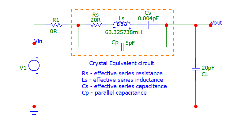
The equivalent circuit is supplied by the crystal manufacturer. It can be used in the following circuit to reveal the crystal's impedance. The values chosen are typical of a common crystal but, I've adjusted Ls to produce series resonance at very close to 10,000,000 Hz. I'm choosing 10 MHz because it's a nice round number and is typical of many crystals: -
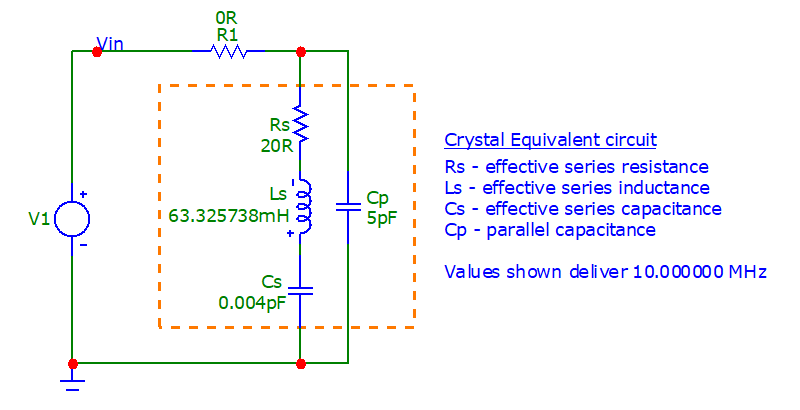
Using this formula: \(\dfrac{1}{2\pi\sqrt{Ls\cdot Cs}}\), the series resonance is 10,000,000.1403 Hz
- R1 is a component fixture used to measure current
- Hence, \(Z_{IN} = V_{IN} ÷ I_{R1}\)
- V1 excites the circuit
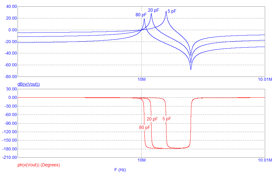
\(\boxed{\text{Here's the impedance plot: -}}\)
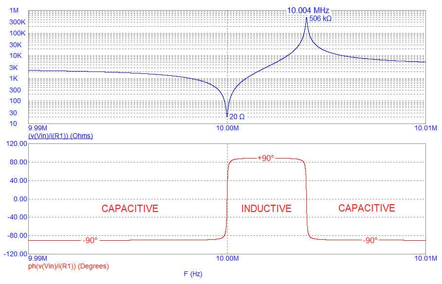
- The x-axis is between 9.99 MHz and 10.01 MHz (chosen for convenience).
- The upper graph (blue) shows that the series impedance is 20 Ω at precisely 10 MHz.
- This corresponds with Rs (the equivalent circuit series resistance).
- Below 10 MHz, the impedance phase angle (red) is -90°. This is regarded as a capacitive impedance.
- Immediately above 10 MHz the phase angle has risen to +90°. This is regarded as an inductive impedance.
- As frequency edges past 10 MHz, the impedance (blue) is steadily rising but the phase angle (red) remains at +90°.
- At 10.004 MHz, the impedance reaches its maximum (about 506 kΩ).
- Above 10.004 MHz, the phase rapidly reverses back to -90°. This is regarded as capacitive impedance.
\(\boxed{\text{Details very close to 10.000 MHz (series resonance): -}}\)
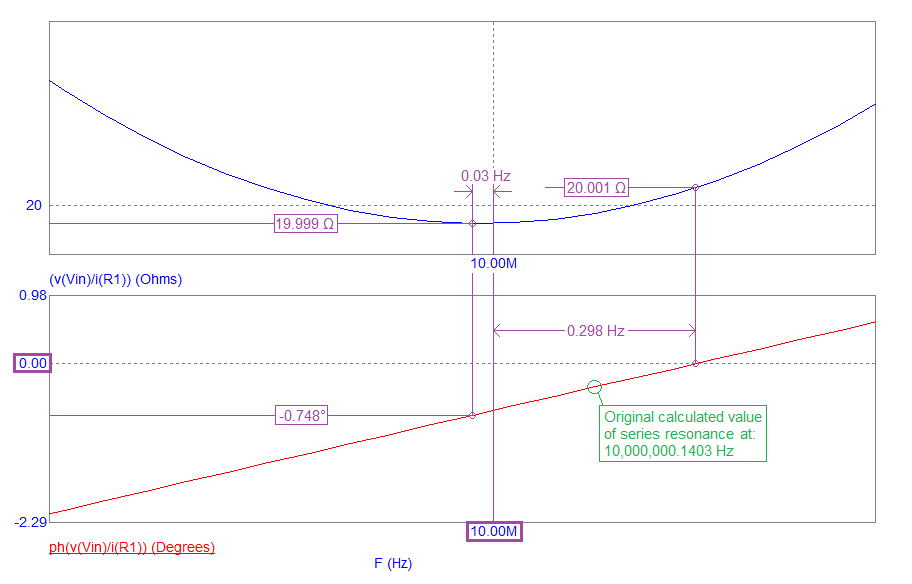
- What we see is that the impedance minimum is actually 19.999 Ω at 0.030 Hz below 10 MHz.
- And, the phase angle is truly resistive at 0.298 Hz above 10 MHz.
- This discrepancy isn't a simulation error but the effect of Cp being in parallel with Rs.
- Rs is the only significant series component due to Ls and Cs cancelling their impedances entirely.
- Ls was chosen to produce series resonance at 10,000,000.1403 Hz but immediately, we see that Cp alters things slightly.
- This general area is called the crystal's series resonant frequency and is, strictly speaking, defined when the crystal's impedance is purely resistive (at 10,000,000.298 Hz).
\(\boxed{\text{Details very close to 10.004 MHz (parallel resonance): -}}\)
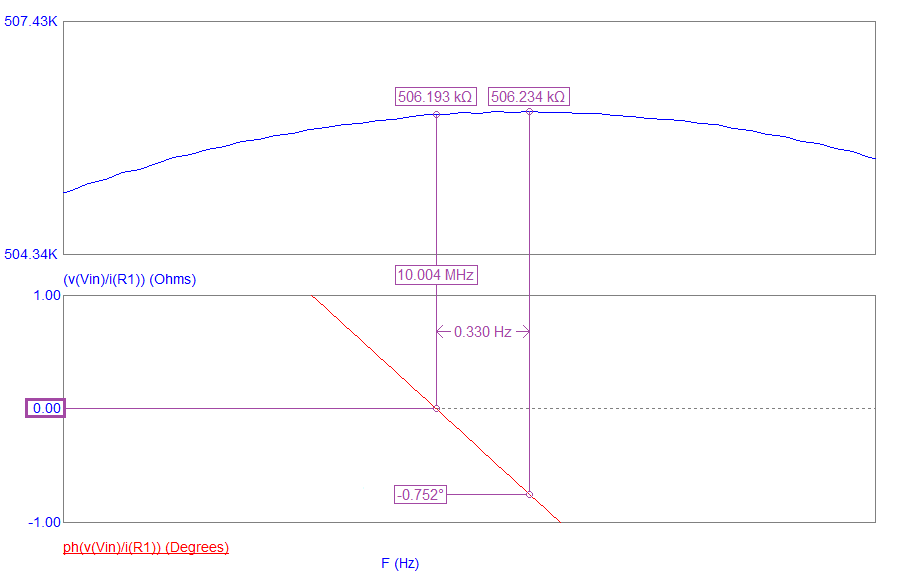
- The impedance amplitude peak value is 506.234 kΩ and is generally referred to as "parallel resonance".
- But, it doesn't quite align with an ideal 0° phase angle.
- The frequency where the phase angle is 0° is sometimes referred to as "anti-resonance".
- The delta frequency that separates parallel and anti-resonance is only 0.330 Hz.
- Parallel resonance is due to the series components Ls and Cs "offering" a small net inductance (above series resonance) and, that little bit of inductance, is in parallel with Cp. Hence, it's a high impedance.
So, if you took Cp (5 pF) and used a calculator to work out what inductance causes parallel resonance at 10.004 MHz you'd get a value of 50.62 µH. This value represents the difference impedance between Cs and Ls at 10.004 MHz and, because the frequency is above 10 MHz, we know that it is net inductive.
However, the large majority of crystal oscillator circuits (such as the Pierce Oscillator), "run" closest to series resonance and, this will be focussed on. Parallel resonance is of some interest but, series resonance is the more important mode for most common oscillators.
To create an oscillator, we should investigate the crystal's transfer function when terminated in a loading component (such as CL below). For the oscillator to be stable, it is desirable that the transfer function produces an unambiguous and reproducible phase angle at just one frequency: -
For various values of CL we see these bode-plot responses: -
- At low and high frequencies, the bode-plot phase response is 0°. Not useful for an oscillator.
- At just above 10 MHz, the phase response falls to nearly 180°. Again not useful for an oscillator.
- The most useful phase angle is -90°. The phase response is steepest and has the least ambiguity.
- However, -90° is not a very useful phase angle for an oscillator that uses an inverting gate to provide gain.
- If we wished to use the crystal in an oscillator, ideally, we need the phase to unambiguously pass through 180°.
For this reason, we use a capacitor on each side of the crystal and a series resistor. The resistor and one of the capacitors produces extra phase shift and pulls the response unambiguously through 180°. In effect, the phase plot (above) is shifted so that the steep vertical lines of the response unambiguously (and conveniently) pass through 180°. This is described below.
You may have seen in crystal data sheets that manufacturers refer to "load capacitance" and recommend a value roughly in the region 5 pF to 30 pF so, let's see what happens when the crystal is "loaded" at both ends (CL1 and CL2). The schematic is this: -
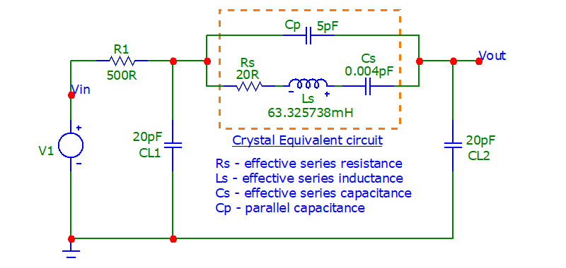
CL1 and CL2 are jointly varied from 5 pF to 30 pF in increments of 5 pF: -
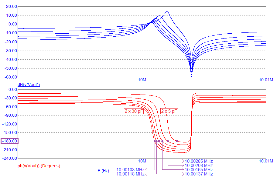
- With 2 x 5 pF of loading, the frequency that produces 180° is less clear than when 30 pF loading capacitors are used.
- The ambiguity arises because the phase response slope is shallower compared to when loading with 30 pF capacitors.
- For example, with 5 pF loading, the frequency of the 180° phase point is 77 Hz higher than when loading with 10 pF.
- Compare this with the frequency difference when the loading changes from 25 pF to 30 pF - it is only 15 Hz.
- In other words, to obtain better frequency stability, you should use larger value loading capacitors.
- However, the correct loading capacitance will be specified by the crystal manufacturer and, this should be used but...
Question: Why not use higher value load capacitors and get better stability?
Answer: It's all down to the allowable power dissipation of the crystal. See this section further down. It's a trade-off.
Manufacturer's normally specify the net load capacitance i.e. if they state 10 pF, then use 2 x 20 pF because the series combination of two 20 pF capacitors is 10 pF. The reason why they state the net load capacitance is for situations where you might want to use one capacitor of 30 pF and another capacitor of 15 pF. There are some circuits (usually BJT oscillators) that can require different values.
RECAP
The crystal by itself may be series resonant at precisely 10 MHz but, for an oscillator circuit, we are interested in the 180° point in the transfer function. In a Pierce Oscillator circuit (using an inverting gate as an amplifier), the crystal circuit "provides" the extra 180° to produce an overall phase shift of 0°. Only this condition creates oscillation and fulfils part of the Barkhausen Stability Criterion.
Previously we fixed the drive resistance at 500 Ω and looked at the effect of varying the loading capacitors. This time we'll keep the loading capacitance at 20 pF and vary the drive resistor (R1) from 250 Ω to 1500 Ω: -
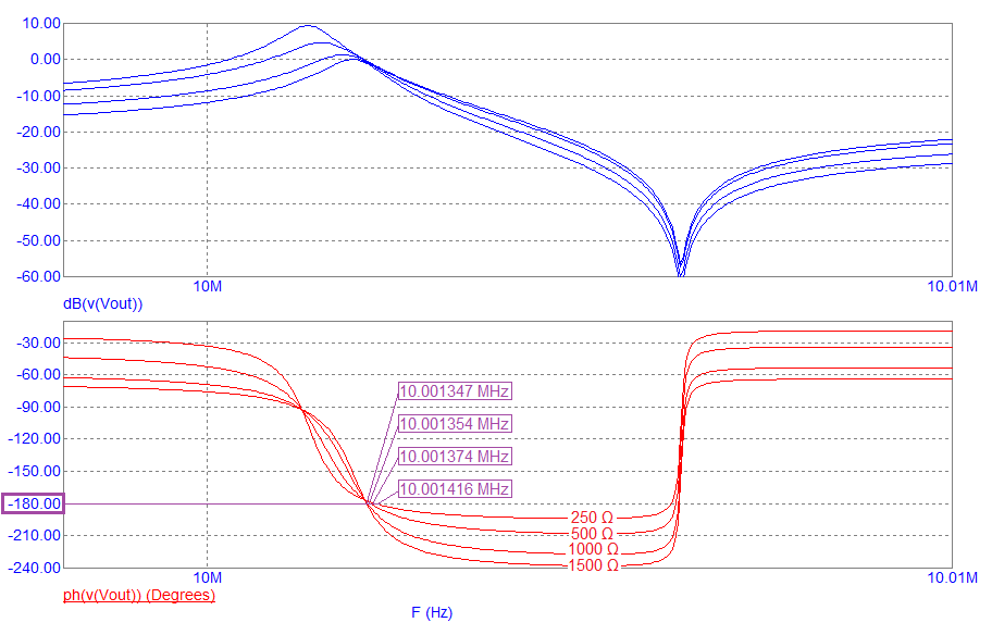
The responses all cross 180° at close to the same frequency so, the effect on oscillation frequency is marginal compared to the effect of loading capacitance changes. However, the steepness that which they cross 180° varies. With a higher value drive resistor (R1), the frequency that produces 180° is less ambiguous. This means better frequency stability.
Many crystal circuits (typically those operating with 32.768 kHz crystals) have a drive resistance of many tens of kΩ. This improves frequency stability and, keeps power requirements down to lower levels (useful for battery powered equipment).
With loading capacitors of 2 x 20 pF, the oscillation point (180°) occurs at 10.00137 MHz. If we replace the crystal's series components (Rs, Ls and Cs) with 16.882246 µH and compare results we see this: -
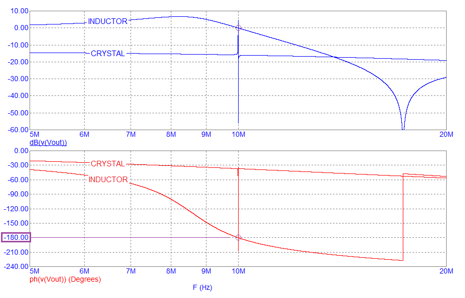
The plots appear dissimilar until you focus on the purple circle at -180°. Each plot crosses 180° at 10.00137 MHz hence, the equivalent series inductance (Le) required to produce 180° phase shift with 15 pF is 16.882246 µH. As a simple check, if you used the well-known formula for LC resonance and plugged in 10.00137 MHz and 15 pF, you'd get an inductance value of 16.882238 µH rather than 16.882246 µH. This latter value, when used in the resonance formula yields a frequency of 10.001367 MHz. The difference is slight.
The 15 pF value is from the series circuit of the 20 pF loading capacitors (CL1 & CL2) being parallel with 5 pF (Cp) hence, 10 pF + 5 pF = 15 pF (Ce)
Many crystal manufacturers specify the maximum allowable power that can be used with their devices. This maximum power, along with the stated loading capacitance, are inter-related. Consider the current that flows in the series element Rs at the oscillation frequency. We can simulate this and plot power dissipation in Rs (pd(Rs)): -
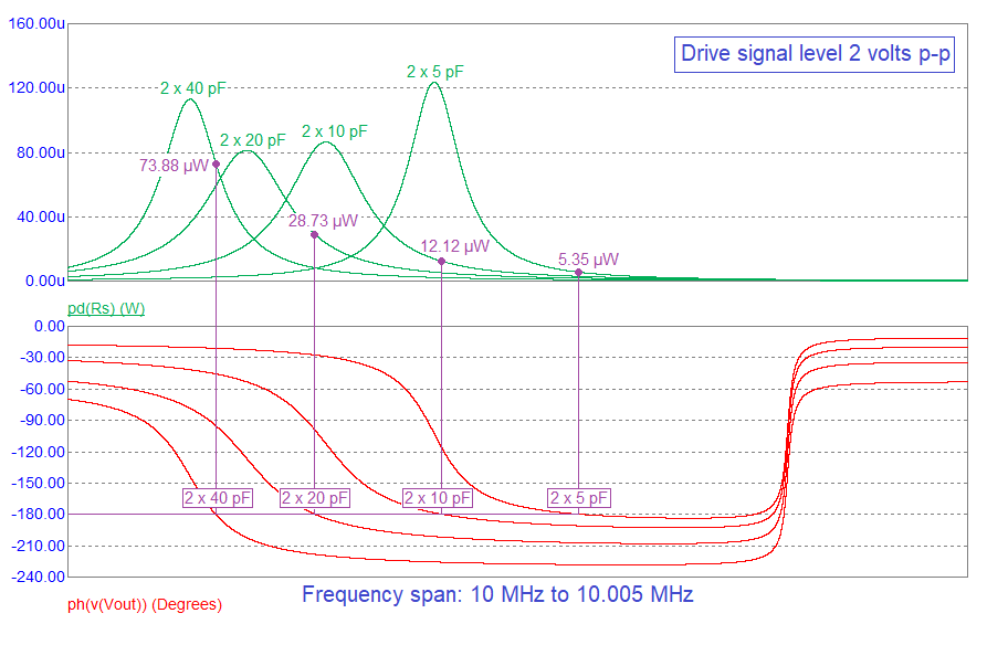
The power figures above are at their respective oscillation frequencies (as dictated by a phase angle of 180°). The power figures are at a drive level voltage (Vin) of 2 volts peak-to-peak feeding via 500 Ω (R1). This is the default value for the simulation AC analysis. The upshot is; if you increase load capacitance, the crystal's power dissipation becomes higher. More heat means a greater likelihood that the crystal accuracy is undermined. A higher drive level means more heat.
No matter how good the crystal is, or how carefully you have chosen the component values around it, if the inverter gate is a poor performer, you will get oscillation frequency errors and possibly excessive frequency drift. Consider the 74AC04 inverter: -
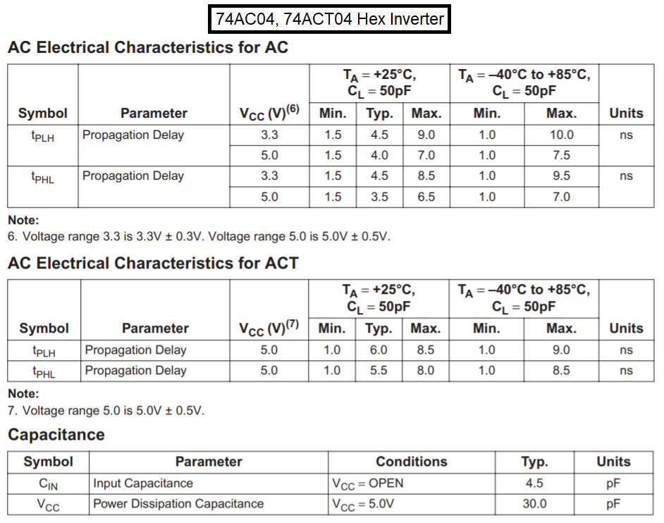
The propagation delay figures quoted for rising and falling edges are typically around 5 ns but could be as high as 10 ns. This means an overall output delay time of 10 ns and, considering that we are looking at a 10 MHz oscillator, 10 ns is equivalent to adding 36° of phase shift. This is alleviated by the type of circuit used; we are operating the gate in a semi-linear fashion and, deep saturation of the output MOSFETs would not happen but, something like 20° of equivalent phase shift might be expected.
This means that the loaded crystal circuit only has to produce a phase displacement of 160° in order to create oscillation: -
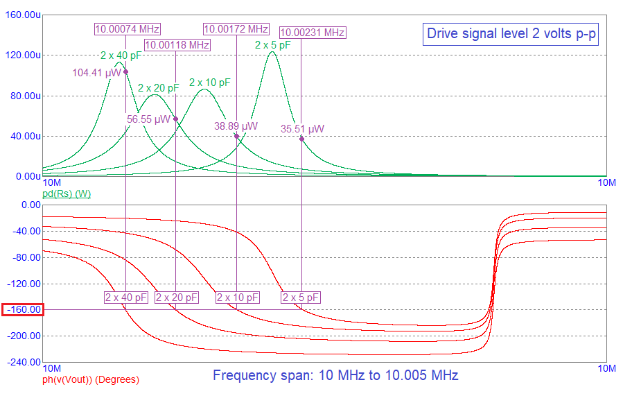
Summary of the effects of a gate delay equivalent to 20°
| Loading capacitance | Gate delay ≡ 0° | Gate delay ≡ 20° | ||
| Required crystal shift: 180° | Required crystal shift: 160° | |||
| Frequency | Power | Frequency | Power | |
| 2 x 5pF | 10.00285 MHz | 5.35 μW | 10.00231 MHz | 35.51 μW |
| 2 x 10 pF | 10.00208 MHz | 12.12 μW | 10.00172 MHz | 38.89 μW |
| 2 x 20 pF | 10.00137 MHz | 28.73 μW | 10.00118 MHz | 56.55 μW |
| 2 x 40 pF | 10.00082 MHz | 73.88 μW | 10.00074 MHz | 104.41 μW |
If the gate propagation delay is temperature dependent, then you will get a small frequency drift with temperature. So, if you are considering using a 74AC04 inverter, be aware of the limitations in terms of frequency accuracy and also be aware of the increased power dissipated in the crystal.
A device that is tailored to crystal oscillators is the SN74LVC1404 (Oscillator Driver for Crystal Oscillator or Ceramic Resonator). It has a propagation delay (between Xin and Xout) of no more than 1.8 ns on a 5 volt supply and no more than 2.4 ns on a 3.3 volt supply. It also has an in-built gate for buffering Xout like this: -
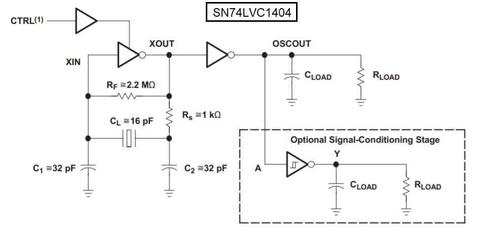
I wouldn't expect this device to produce a delay that incurred anything more than a 4° phase shift at 10 MHz.